| SCHIBLI−LAB AT THE UNIVERSITY OF COLORADO |  |
||
|---|---|---|---|
| We make light shine! | |||
| Graphene-based optical materials & devices | |||||||
|
While graphene—single-atomic-layer graphite—has existed a long time as a theoretical construct (or more recently also here), it was only recently that graphene was actually discovered in the laboratory. It garnered an enormous amount of interest - so much interest, in fact, that some of the pioneering researchers on graphene won the Nobel Prize in Physics, 2010. This interest stems from graphene's many extraordinary properties. Graphene is a fantastic conductor, allowing for sheet resistance as low as 125 Ohms/Square. As shown in the figure 2 on the right it is a zero-bandgap semiconductor with linear band structure near the k-point. This unique band-structure gives graphene a universal 2.3% linear optical absorption that makes it transparent, despite its high conductivity. Now there is active research in using graphene as a transparent electrode for flexible touch screens, as a material in high-speed transistors, and in many more applications. Furthermore, graphene is nature’s closest approximation to a true two-dimensional material, since it is only a single atom thick—which lets us use it to experimentally probe fundamental physics. Our interest in graphene focuses on the optical and opto-electronic applications of this novel material. We are currently working on a graphene-based broadband saturable absorbers for femtosecond pulse generation (Fig. 2-4), for Quantum Interference Control (QIC) devices (Fig. 5-6), and graphene-based electro-optic modulators. Graphene synthesis We produce our graphene by low pressure chemical vapor deposition (LPCVD) on copper, such as previously reported here, and here. At high temperatures up to about 1300 K and low pressures (below 10 mTorr), we flow methane or acetylene gas over copper foil. The foil catalyzes the breakdown of the gas into carbon and hydrogen. The carbon deposits itself on the exposed copper foil as a honeycomb lattice, while the hydrogen difuses away. Because exposed copper is required to catalyze the reaction, growth self-terminates when a single atomic layer of carbon covers the whole copper surface. We then etch the underlying copper away and transfer the graphene onto an arbitrary substrate, where it is held in place due to Van der Waals forces. 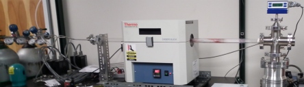 Our home-build low-pressure CVD system delivers high-quality, large-area single atomic layer graphene sheets on copper surfaces. Ultrafast optical properties Optically, one of the most interesting features of graphene is its universal 2.3% absorption over every wavelength of light. Furthermore, as a semiconductor, the optical absorption of graphene saturates at high light intensities. The wavelength-independent saturation of optical absorption is shown in the figure 2: At low intensities graphene absorbs 2.3% of the light passing through it. At high optical intensities the photo-generated carriers block further absorption. This effect can be used to shorten optical pulses: As an optical pulse travels through the graphene, the low-intensity pulse “wings” are attenuated by the graphene's absorption more than the high-intensity pulse center (see Fig. 4). This enables novel ultra-broadband mode-locking devices for solid-state, as well as fiber lasers to produce pulses mere femtoseconds wide and of any color of light. Mode-locking with graphene is particularly interesting for new types of long-wavelength light sources, such as chip-scale lasers, and also for novel Mid-IR laser sources based on thulium-doped glasses or chromium-doped II-VI semiconductors. Such Mid-IR sources would open up new avenues for ultra-sensitive molecular detection. Graphene electro-optic modulators While we can change the optical absorption of a graphene sample by saturating it with laser light, we can also use chemical or electro-static doping. As shown in the figure 7, a change in the fermi level can be used to block the optical absorption. Instead of chemical doping one can also use electro-static doping similar as in a field effect transistor (FET). Electro-static doping enables graphene-based electro-optic modulation of light. Unlike most modulators, however, a graphene-based device is ultra-broadband and produce little to no signal distortion or dispersion as an optical pulse travels through them. We have successfully used such modulators to stabilize optical frequency combs with record-low residual phase noise. |
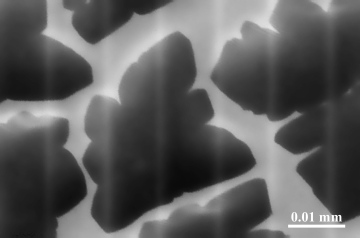 Fig. 1: SEM image of a single-atomic layer graphene crystal on copper surface. The flake was grown in our CVD setup at moderately low pressure (~10 mTorr). With even lower pressures we have obtained single cristaline flakes measuring more than 0.1 mm on each side. |
||||||
| A
single atomic layer of graphene is visible to the naked eye, as it
shows a wavelength- independent absorption of a whopping 2.3%. |
|||||||
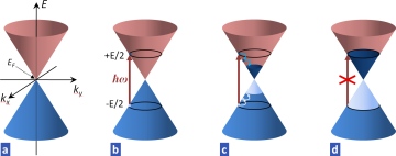 Fig. 2: Saturation of optical absorption in graphene: A. Conical low-energy spectrum E(k) of graphene. Blue: filled valence band; Red: empty conduction band. B. Optical absorption of a photon with energy E=ħω. The vertical arrow indicates an interband transition. C. Thermalization of photo-generated carriers (<1 ps). D. At high optical intensities the photo-generated carriers block further absorption.  Fig. 3: Large area, ultrabroad-band saturable absorber mirror based on single layer graphene. Such mirrors are used in our group for mode-locking compact solid-state lasers. 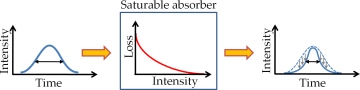 Fig. 4: Pulse shortening by saturable absorption: when passing through a saturable absorber, the low-intensity wings of a pulse experience higher loss than the intense pulse center, which results in a shorter pulse.  Fig. 5: Quantum interference control (QIC) detector based on single-layer graphene. Such detectors could allow for direct detection of the carrier-envelope phase evolution in ultrashort optical pulses. 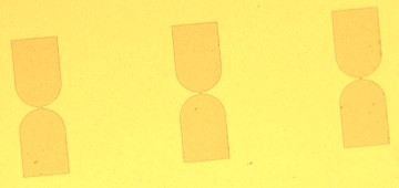 Fig. 6: Actual QIC devices manufactured in our lab. The graphene bridge between the electrodes is approximately 10 micrometers long. The 400 micron long pads are used to attach electrical connections to the device. 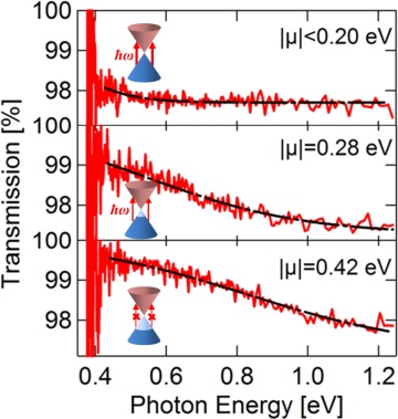 Fig. 7: Effect of the Fermi-level in graphene on its optical absorption: With a Fermi-level close to the dirac point, the optical transparancy (y-axes) of graphene shows little wavelength dependence. With a Fermi-level shifted by at least half the photon energy (x-axes) graphene becomes highly transparent.  Fig. 8: left: integrated graphene electro-optic modulators; right: measured modulation depth across a single graphene modulator. |
|||||||
| <Back |
|||||||