| SCHIBLI−LAB AT THE UNIVERSITY OF COLORADO |  |
||
|---|---|---|---|
| We make light shine! | |||
| Chip-scale mode-locked lasers | ||||||
|
Lasers
that produce pulses with femtosecond durations (1 fs = 10-15s)
have found a large
variety of scientific and commercial
applications. Length, distance and optical frequencies are
now
routinely measured with fs-lasers. Optical frequency combs produced by
fs lasers are key technology to probe and manipulate
the quantum state
of atoms or molecules, and in vivo 3D imaging with micrometer
resolution is achieved by optical coherence tomography using fs-lasers
as light sources. Fs pulses are also indispensable for the
investigation of electron dynamics in solid-state materials, such as in
novel nano-structured metamaterials.
An increasing number of applications require local oscillators with ultra-low timing jitter. An example of these applications is ultra-high speed analog to digital conversion (ADC), which is extensively used in software defined RADAR and radios. The performance of such high-speed ADCs is ultimately limited by the timing jitter and power of their local oscillators. For example, a 12 bit ADC at a 10GHz input frequency requires a timing jitter of less than 4 fs. This low jitter cannot be obtained by state-of-the art room-temperature microwave oscillators but it is possible to achive sub-fs jitters with actively stabilized optical frequency combs. Our chip-scale mode-locked lasers project targets the development of monolithic femtosecond sources based on integrated optics, ultimately leading to fs-lasers on a chip. Such sources enable not only a dramatic reduction in size but also a vastly improved immunity against environmental influences. This leads to mode-locked lasers that operate close to the quantum limit. Such sources could find their way in our households similar to the cw-laser diodes some thirty years ago. Mode-locked semiconductor lasers certainly would qualify for applications outside the protected environment of the optics laboratory. However, their performance is severely restricted by the short lifetime of the gain inversion (typically 10 ns or less). Compact and rugged fiber lasers on the other hand have recently proven suitable for precision optical measurements and for generating fs-combs at the highest level of precision, but none of these systems qualify for integration in an instrument nor could they be operated by laypersons. A variety of applications we are foreseeing for these sources are:
Challenges: Making
state-of-the-art solid-state lasers smaller brings a variety of
challenges. Two of the most severe challanges are material damage
(especially if III-V semiconductor absorbers are used), and dynamic
instabilities, such as Q-switching instabilities. Both of these issues
are related to the high repetition rate, and the limited intracavity
pulse energy in compact lasers. Latter can be overcome by passive means
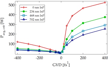
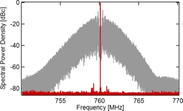
(namely intra-cavity dispersion management, and inverse saturable absorption; see Fig. 3), or by active feedback methods (see Fig. 4).
To overcome both, the material damage and Q-switching issues, we have developped graphene-based saturable absorbers, that enable active modulation of the intracavity loss, as well as passive mode-locking owing to the intrinsic saturable loss of graphene. |
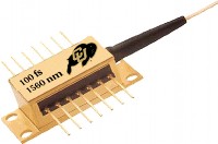
 Fig. 1: Artist’s vision of a fully integrated and packaged fs-laser. Control-electronics in form of a CMOS chip could also be integrated in the same package. |
|||||
| Chip-scale
mode-locked lasers [...] could find their way in our households similar
to the cw-laser diodes some thirty years ago. |
||||||
 Fig. 2: Schematic diagram of a monolityic solid-state laser based on rare-earth-doped glass. The laser is mode-locked by a graphene-based, laterally coupled saturable absorber/modulator for mode-locking and Q-switching suppression.  Fig. 3: Required intracavity average power to overcome Q-switching for a 10GHz fundamentally mode-lockd Cr:YAG laser. The data is obtained from a numerical simulation, and is ploted as a function of intracavity dispersion. The numbers in the legend indicte the thickness of an intracavity InP layer (two-photon absorber).  Fig. 4: Active stabilization of a high-power, high-repetition rate Nd:YVO4 laser pumped with a laser diode bar. Gray: no active stabilization: laser is Q-switching. With active stabilization (red): laser operates in the continuous mode-locking regime. The feedback acted solely on the pump-current of the diode bar. |
||||||
| <Back |
||||||